MICROELECTRONIC ASSEMBLY
IC ASSEMBLY: BACK END
DIE PREPARATION
Dicing
Dicing is the process by which the wafer is singulated into individual dice in preparation for assembly. The dicing process consists of two major steps; wafer mounting and wafer sawing. MAK can perform dicing of reticles, wafers and substrates mounted on up to 8” dicing rings. Larger wafers are outsourced, all communication is handled, if requested, by MAK.
Back grindning
Wafer Backgrind is the process of grinding the backside of the wafer to the correct wafer thickness prior to assembly. MAK does not have backgrinding inhouse, but we will outsource and handle all communication if requested.
IC PACKAGES
Open Cavity packages that we can handle:
• DIP
• MLF / MLP / QFN / DFN / LPCC
• PLCC•SOT / SC / TO / DPAK
• QFP / LQFP / PQFP / TQFP
• SSOP / TSOP / TSSOP
• SOIC / SOJ / MSOP / QSOP
• SOT / SC / TO / DPAK
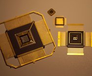
Ceramic Packages are available with a variety of lids including taped-on, ceramic, glass and hermetically sealed.
M A Kapslingsteknik can provide virtually any package you need for your prototype devices, such as open cavity, ceramic, laminate substrates and even custom package configurations.
If you don’t have a specific package identified, we can provide technical assistance to select the best package for your application.
Open Cavity Packages
Open Cavity Packages are the ideal platform for new IC prototypes, because they are mechanically and electrically identical to your future transfer moulded production parts. We can work with industry standard open cavity packages from most major suppliers, we can also assist in purchasing them for your need.
Ceramic Packages
MAK can provide a full turnkey solution when ceramic packages are the right choice for your prototype devices. We will source packages from industry-leading ceramic suppliers and assemble your devices according to your specifications.
Laminate Substrates
If your product calls for the development of a custom BGA, interposer or other laminate substrate along with assembly services, MAK is the answer. We will coordinate the design and fabrication of your substrate, attach and wire bond your die, encapsulate, mark and attach the solder spheres.
We have developed our own line of laminate based MLF / MLP / QFN / DFN that are ideal for fast prototyping and low to medium volume products.
We have qualified substrate suppliers that can manufacture substrates with the latest technology. Outline and performance is identical to lead frame based packages.
Lead Frames
MAK can offer custom lead frame designs for volume production as well as for prototypes. We often work with fully plated (Ni/Pd/Au) lead frames in order to eliminate the post moulding plating process.
Laminate Substrates
Custom lead frames
IC ASSEMBLY: BONDING
Adhesive bonding
Adhesive bonding is done with special conducting or non-conducting adhesives depending on application demands.
Wire Bonding
There are few companies in Northern Europe that can match MAKs’ wire bonding knowledge and experience. Gold ball bonding is our main stream wire bond technology. Standard pitch is 50 µm, but for prototypes the pitch can be decreased.
Other bonding methods available at MAK are
• Soldering
• Vacuum soldering
• Micro welding
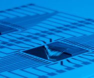
General:
• Wire diameter 17 µm - 75 µm
• Short wires < 300 µm
• Long wires > 10 mm
• Stacked die
• Multi-die
• Multi-tiers
Ball bonding:
• Gold ball bonding
• Stud bumping (Au-wire)
Wedge bonding:
• Gold wedge bonding
• Aluminum wedge bonding
• Heavy wires:
125-500 µm Au, Al, Pt
Micro welding
IC ASSEMBLY: ENCAPSULATION
Encapsulation Options
After wire bonding, MAK offers several options for encapsulation of your devices, providing the level of protection and/or accessibility that you need. Options include:
Fully Encapsulated
Transfer moulded: Packages are fully encapsulated with epoxy with our industry standard moulding process.
PMM: Packages are fully encapsulated with epoxy, utilizing MAK developed moulding process. Packages are providing test socket compatibility.
Glob Top: Packages are fully encapsulated with silicone or epoxy and have a domed surface.
Clear Epoxy: Packages are fully encapsulated with non-filled epoxy as Glob Top or with PMM, for bonding verification, visual samples and optical applications.
Hermetic: For more demanding applications we can provide hermetic seam welded packages according to MIL standards.
Partially Encapsulated, Exposed Die
Packages are encapsulated with epoxy or silicone in selected areas.
Open
If requested we can also ship packages in protective boxes with die and bond wires exposed
PMM
Fully Encapsulated
Glob Top
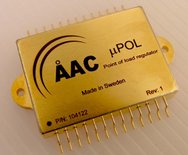
Hermetic seam seal welded package
IC ASSEMBLY: ADDITIONAL
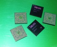
BGA spheres attached on the back of the component
BGA Ball Attach
MAK can attach BGA spheres to your custom substrates. Spheres in sizes from 0.25 mm to 2.00 mm are available in both Sn/Pb and Pb-free alloys.
MAK can attach spheres to new modules or can rework an existing module.
Flip Chip Assembly
MAK has Flip Chip bonding capability and can place bumped devices within +/- 10 µm placement accuracy.
Applications include flip chip, 3-D packaging, MEMS, optoelectronic and micro optics bonding and assembly, sensors, chip on glass/chip on flex and more.
Test
MAK have the knowledge and experience to offer testing of components after assembly. The customer needs to provide product specific test devices for electrical test, MAK provide the test handler and the operator and will run the process with full engineering support.
Reliability testing
When it is time for reliability testing of your products, MAK have the equipment in place to offer following reliability tests:
• Temperature Humidity Bias (THB) Life Test 85°C/85% relative humidity - JESD22-A101
• Moisture/Reflow Sensitivity Classification - IPC/JEDEC J-STD-020
• HTSL (High-Temperature Storage Life Test) - JESD22-A103, MIL-STD-883 Method 1008
• Temperature Cycling (TC) Air to Air - JESD22-A104, MIL-STD-883 Method 1010.7
• Preconditioning - JESD22-A113
Tape and Reel
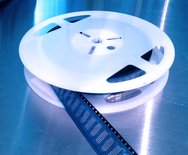
MAK can provide packages in waffle pack, Jedec trays, bags or tape and reel. The tape and reel process can handle tape from 8 to 72 mm according to EIA-481. This service is only offered in combination with any of our other services.
Laser Marking
Marking your completed devices after encapsulation or lid attach is the ideal way to ensure proper identification, whether you are performing internal testing or shipping customer samples. With our laser marker we can make company logo, company name, product name, lot number, wafer number, serial number or date code.
We can work with most image formats and can assist in creating custom artwork to meet your marking needs.
Jedec tray
The encapsulated components can be put in tape & reel for protection and easy handling in mounting machines. Tape width 8-72 mm
Laser marked components packed in Waffle Pack
ADVANCED MICROELECTRONIC ASSEMBLY
The flexible processes and equipments of MAK makes it possible to deliver prototypes that fulfil the advanced assembly requirements of for example Flip Chip, Chip-on-Board, Stacked die, Multi-Chip Modules, System-in-Package, BGA and MEMS devices.
Chip on Board (COB) / Chip on Flex (COF)
MAK has the capability to attach and bond dies on printed circuit boards and flex circuits. Passive components can be mounted and die protected with encapsulation, frame and lid or custom covers. MAK also has the capability of designing unique test fixtures for your populated boards.
Multi-Chip Module (MCM) / System in Package (SiP)
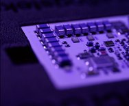
MAK’s flexible assembly processes can accommodate the bonding of multiple components, including die and discretes, on substrates. MAK can supply a turn-key solution, source ceramic or laminate based substrates from industry-leading suppliers and assemble your module according to your specifications
Flip Chip Bonding
When you are ready to make the move to Flip Chip technology, MAK offers complete prototype assembly services, including:
• Die Bumping
• Die Placement
• Solder Reflow
• Underfill
• Encapsulation
• Substrate Ball Attach
MAK also provides substrate design and manufacturing services to deliver a complete turnkey Flip Chip solution.
Stacked Die
When your device requires the integration of multiple components in a single package, such as ASIC and memory die, a stacked die assembly delivers the smallest footprint and most economical solution. Our capabilities in die attach and wire bonding, including die to die and die to substrate bonding, enable prototype assembly of your complicated stacked die devices. Back-grinding of individual dies enables the finished devices to meet original JEDEC package thickness specifications.
MEMS
MAK’s assembly techniques and our knowledge in polymeric materials provides the capability to assemble unique MEMS devices, including chemical, environmental and pressure sensors and other configurations requiring an air cavity.
Multi-Chip Module

M A Kapslingsteknik AB
Maskinvägen 6
746 30 Bålsta
Sweden
Copyright 2018 @ All Rights Reserved
